- 您现在的位置:买卖IC网 > Sheet目录481 > MTP10N10ELG (ON Semiconductor)MOSFET N-CH 100V 10A TO220AB
�� �
�
�MTP10N10EL�
�12�
�Q� T�
�90�
�75�
�1000�
�T� J� =� 25� °� C�
�I� D� =� 10� A�
�V� DS� =� 100� V�
�8�
�V� GS�
�60�
�100�
�V� GS� =� 5� V�
�t� r�
�45�
�t� f�
�4�
�Q� 1�
�Q� 2�
�T� J� =� 25� °� C�
�30�
�10�
�t� d(off)�
�t� d(on)�
�I� D� =� 10� A�
�15�
�0�
�0�
�2�
�Q� 3�
�4�
�6�
�V� DS�
�8�
�0�
�10�
�1�
�1�
�10�
�100�
�Q� G� ,� TOTAL� GATE� CHARGE� (nC)�
�Figure� 8.� Gate?To?Source� and� Drain?To?Source�
�Voltage� versus� Total� Charge�
�R� G� ,� GATE� RESISTANCE� (OHMS)�
�Figure� 9.� Resistive� Switching� Time�
�Variation� versus� Gate� Resistance�
�DRAIN?TO?SOURCE� DIODE� CHARACTERISTICS�
�10�
�8�
�6�
�4�
�2�
�0�
�V� GS� =� 0� V�
�T� J� =� 25� °� C�
�0.5�
�0.6�
�0.7�
�0.8�
�0.9�
�1.0�
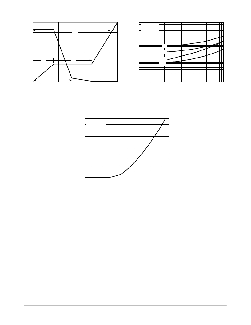
�V� SD� ,� SOURCE?TO?DRAIN� VOLTAGE� (VOLTS)�
�Figure� 10.� Diode� Forward� Voltage� versus� Current�
�SAFE� OPERATING� AREA�
�The� Forward� Biased� Safe� Operating� Area� curves� define�
�the� maximum� simultaneous� drain?to?source� voltage� and�
�drain� current� that� a� transistor� can� handle� safely� when� it� is�
�forward� biased.� Curves� are� based� upon� maximum� peak�
�junction� temperature� and� a� case� temperature� (T� C� )� of� 25� °� C.�
�Peak� repetitive� pulsed� power� limits� are� determined� by� using�
�the� thermal� response� data� in� conjunction� with� the� procedures�
�discussed� in� AN569,� “Transient� Thermal�
�Resistance?General� Data� and� Its� Use.”�
�Switching� between� the� off?state� and� the� on?state� may�
�traverse� any� load� line� provided� neither� rated� peak� current�
�(I� DM� )� nor� rated� voltage� (V� DSS� )� is� exceeded� and� the�
�transition� time� (t� r� ,t� f� )� do� not� exceed� 10� m� s.� In� addition� the� total�
�power� averaged� over� a� complete� switching� cycle� must� not�
�exceed� (T� J(MAX)� ?� T� C� )/(R� q� JC� ).�
�A� Power� MOSFET� designated� E?FET� can� be� safely� used�
�reliable� operation,� the� stored� energy� from� circuit� inductance�
�dissipated� in� the� transistor� while� in� avalanche� must� be� less�
�than� the� rated� limit� and� adjusted� for� operating� conditions�
�differing� from� those� specified.� Although� industry� practice� is�
�to� rate� in� terms� of� energy,� avalanche� energy� capability� is� not�
�a� constant.� The� energy� rating� decreases� non?linearly� with� an�
�increase� of� peak� current� in� avalanche� and� peak� junction�
�temperature.�
�Although� many� E?FETs� can� withstand� the� stress� of�
�drain?to?source� avalanche� at� currents� up� to� rated� pulsed�
�current� (I� DM� ),� the� energy� rating� is� specified� at� rated�
�continuous� current� (I� D� ),� in� accordance� with� industry�
�custom.� The� energy� rating� must� be� derated� for� temperature�
�as� shown� in� the� accompanying� graph� (Figure� 12).� Maximum�
�energy� at� currents� below� rated� continuous� I� D� can� safely� be�
�assumed� to� equal� the� values� indicated.�
�in� switching� circuits� with� unclamped� inductive� loads.� For�
�http://onsemi.com�
�5�
�发布紧急采购,3分钟左右您将得到回复。
相关PDF资料
MTP12P10G
MOSFET P-CH 100V 12A TO220AB
MTP23P06VG
MOSFET P-CH 60V 23A TO220AB
MTP2955V
MOSFET P-CH 60V 12A TO-220AB
MTP2P50E
MOSFET P-CH 500V 2A TO-220AB
MTP3055VL
MOSFET N-CH 60V 12A TO-220AB
MTP3055VL
MOSFET N-CH 60V 12A TO-220
MTP3055V
MOSFET N-CH 60V 12A TO-220AB
MTP36N06V
MOSFET N-CH 60V 32A TO-220AB
相关代理商/技术参数
MTP10N10M
制造商:Motorola Inc 功能描述:
MTP10N15
制造商:MOTOROLA 制造商全称:Motorola, Inc 功能描述:POWER FIELD EFFECT TRANSISTOR
MTP10N25
制造商:MOTOROLA 制造商全称:Motorola, Inc 功能描述:POWER FIELD EFFECT TRANSISTOR
MTP10N40
制造商:MOTOROLA 制造商全称:Motorola, Inc 功能描述:TMOS POWER FET 10 AMPERES 400 VOLTS RDS(on) = 0.55 OHMS
MTP10N40E
制造商:Rochester Electronics LLC 功能描述:- Bulk
MTP1149
功能描述:触觉开关 SW TACT SPST 0.05A 12VDC
RoHS:否 制造商:C&K Components 工作力:2 N 执行器:Round 电流额定值:50 mA 电压额定值 DC:32 V 电压额定值 AC: 功率额定值:1 VA 接地端子:Yes 触点形式:SPST-NO 开关功能: 安装风格:SMD/SMT 安装方向:Right 晶体管管座高度: 颜色: 照明:Not Illuminated 照明颜色: 封装:
MTP127M030P1C
制造商:MALLOR 功能描述:
MTP12N05E
制造商:MOTOROLA 制造商全称:Motorola, Inc 功能描述:POWER FIELD EFFECT TRANSISTOR